DRPiTOS Part 1: Concepts and Design:
July 31, 2021
Content:
1) Introduction
In the past I've designed a custom operating system as a semester project in college almost 2 years ago. The microprocessor the OS was designed for was a RTOS (Real-Time Operating System) for the ATmega328PB (an 8-bit AVR processor). Not every important feature of the Operating System wwas implemented on that microprocessor (features such as Semaphores and some memory sharing being one feature not implemented) but most of the functionality of an Operating System was there such as I/O Allocation, Priority Scheduling (First Come First Serve Scheduling) and storing Register data onto the stack. The two applications used to test the Operating System was basic applications that involve powering up an LED through a GPIO Pin. Both pins are used for both tasks, of course only one of them at a time was allowed to be used.
The goal of this project is to design a custom operating system for the Raspberry Pi Pico. A $4 embedded system with a RP2040 microprocessor. More information on the specs will be mentioned in the next section though one important thing to note is this microprocessor is a dual core Cortex M0+ CPU which adds a layer of challenge to OS design that the single core ATmega328PB does not have. Of course it's possible get away with only running on one CPU core, however it's important to be able to fully utilize the hardware provided and having two cores means two tasks can be done at once or one can be done at a time while the OS is operating if a task takes more than one systick (See Timers and Task Management Sections).
2) Raspberry Pi Pico Specs
2.1) Microprocessor
The Microprocessor is an RP2040 which is a dual ARM Cortex-M0+ core CPU running at 133 MHz. Assuming each instruction takes one CPU cycle the CPU can perform 133 Million instructions in one second, of course some instructions take more than one instruction. The list of instructions can be found on the Cortex M0+ Generic User Guide.
The RP2040 being a dual Cortex-M0+ means that two instructions at a time can be executed. The benefit to that means higher performance is possible beyond what a single core CPU can run but the downside is the extra difficulty in implementing this in an operating system as the last thing that we want to encounter is overwriting a memory space shared between two CPUs.
2.2) Memory
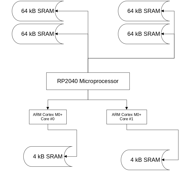
The memory setup (aside from SPI Flash which is 16 MB but for the project I won't be using this for anything extra) is 4 banks of 64 kB SRAM and 2 banks of 4 kB of memory giving us an effective total of 264 kB of SRAM. There are two possible ways to setup the 64 kB banks, either treat them as seperate banks or merge them to make one large 256 kB bank. For the purpose of this project it is more beneficial to treat the four 64 kB memory banks as one large 256 kB memory bank since it will be easier to manage it this way, but this makes little difference either way. In fact, it might also help just as much to read from one memory bank at a time from a performance perspective so maybe having it as four seperate isn't so bad neither, or I could do striped and non-striped operation combos given the memory map proposed. For my proposed OS design I find it more pragmatic to treat it as one large bank (check Section 3.1 and 3.3). The two 4 kB banks can be used one for each CPU core, especially useful if a task manages to take longer than a SysTick (check Section 2.3, 2.4 and 3.3 for more info) and the data of the old task needs to be stored somewhere for the CPU to access.
2.3) Timers
For timers the RP2040 has an array of options compared to the ATmega328PB having only 8-Bit and 16-Bit timers (of course other Interrupts and such could be used to create psuedotimers). For the RP2040 there are five timer options that are of more variety. Such timers include:
- One Global 64-bit timer that's a counter which runs at 1 MHz.
- Eight of the PWM's 16-bit programmable counters which can run up to system speed (133 MHz).
- Eight PIO State MAchines which can count 32-bit values at system speed and generate interrupts.
- Four internal pacing timers
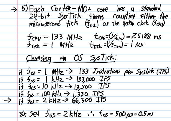
- Two Cortex M0+ timers built to the CPU, one for each core. These are standard 24-bit SysTick timers that count either at a Microsecond tick or the System clock.
Our of all these options, the fifth option is the best one to use as a timer for the Operating System. In terms of the timer we will be counting by the microsecond rather than counting based on the frequency, so the timer runs at 1 MHz rather than 133 MHz however deciding on how far it should count is a different matter and a speed for a SysTick should be decided. For this project, I will set the SysTick to 2 kHz (0.5 ms) for each timer. Given a frequency of 133 MHz for a CPU core that gives an application up to around 66500 Instructions per SysTick at most (though likely will be lower, if an application requires more than 66500 instructions, then it will have to save data till the OS decides it can continue where it left off which will require considerably more amount of instructions). The higher the SysTick the longer the OS takes to respond and the shorter the SysTick the less time the OS takes to respond.
2.4) GPIO
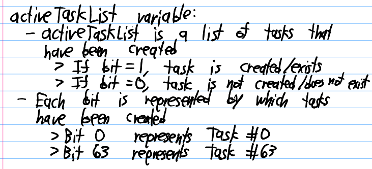
The Raspberry Pi Pico has a total of 29 GPIO pins, pins can be used for input, output or as other sources such as an ADC, SPI, I2C, etc. Some pins such as GP23, GP24 and GP25 are not on the Raspberry Pi Pico board but the pins are on the CPU so for the sake of simplicity I will include those pins as well. Multiple tasks cannot use the same pin at once so a permission system is going to be required and handled by the OS on which tasks are allowed to use the pin and which aren't. Check Section 3.4 for more information on I/O management.
2.5) Registers
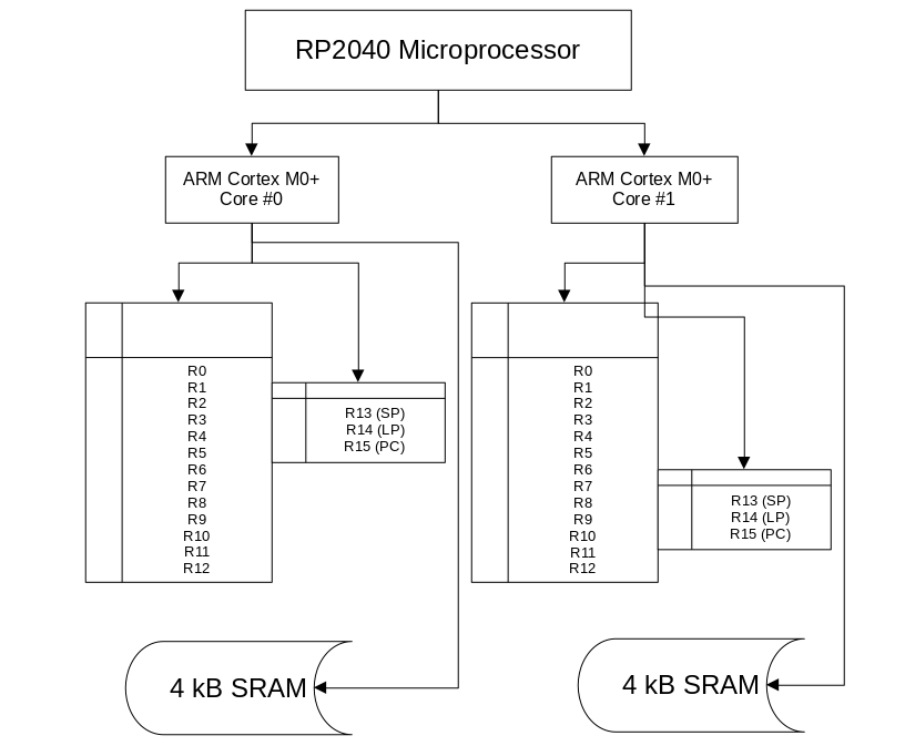
For the Registers there are 13 general purpose registers, 1 register for the Process Stack Pointer, 1 for the Link Register and one for the Program counter. The registers not shown in the diagram include the Program Status Register, PRIMASK register and the Control register, those should also be saved as well. When the system needs to switch between the operating system and tasks, each CPU core must be able to push the data in those registers into a stack of memory so that it can be used when the task switches back. It is uncertain as to whether or not in terms of how to do that will require writing the program and debugging the code until it is certain how data should be saved from the registers to the stack and how to load data from the stack back onto the registers. The Program Counter should be saved first and loaded the last as once the program counter is loaded the CPU goes back to where it left off.
3) Basic Operating System Design
3.1) Memory Management
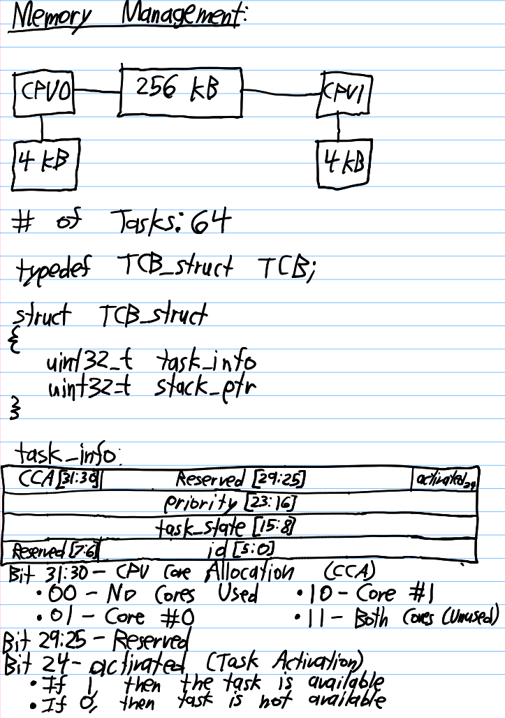
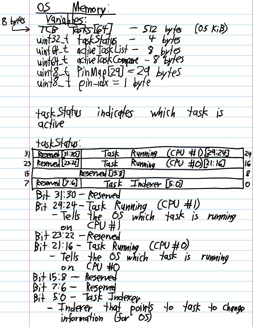
Memory management is going to be the bulk of the work the OS has to do, especially to manage how much memory and when the memory can be accessed. The memory map on the 3rd page shows how the 256 kB of memory allocation will initially be done, although I considered shrinking the OS RAM down to 16 kB and increase the Shared Memory Pool to 48 kB and technically I could go even further on that, but the OS will likely require at least 1 kB. The properties in each task is contained in a data type known as a TCB. Each TCB contains 8 bytes of data and with 64 tasks the total space for the TCB array is 512 bytes (or 0.5 kB). The remaining data takes up 50 bytes total (unless the 8-bit variables get converted to 32-bit variables when stored, in which case, that would take up 140 bytes. This is more than enough memory for the OS.
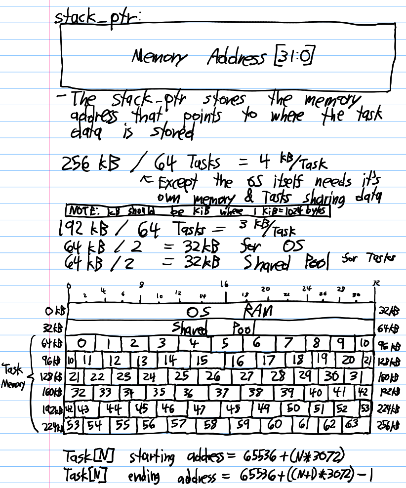
After the OS memory then there is the shared memory, the proposed map shows 32 kB of shared memory is allocated for use for all tasks. The current implementation is that all tasks can access every address on the Shared Memory though a permission system could be considered to determine which addresses go to which tasks. Such information regarding the memory may have to be stored either on the OS or the remaining memory leftover from the Stack Memory, not to mention splitting up the Shared Memory into blocks of their own. If more shared memory is important, then it can be reallocated from the OS's free space and cutting down the size of each memory block from each task down.
The last section of the 256 kB memory block is the amount of memory available for each task. Since 64 kB is used for the OS Memory and Shared Memory the remaining 192 kB is split into 3 kB for each task. 3 kB is plenty of memory for most applications related to microprocessors to be frank and if any more is needed it can call onto Shared Memory. If anything, this is something that could be scaled back in favor of having a larger pool of Shared Memory but it's also important not to scale that back too much. For now this will be the memory map to stick to when making the OS.
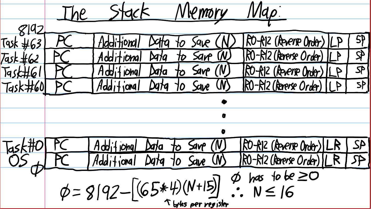

Another challenge is fitting all of that data for 64 Tasks and the OS with the two 4 kB memory banks. Most CPU instructions require using these registers meaning that data has to kept being saved and moved around so that it can all be properly restored so that's more data in addition to 16 Registers that are already to be saved, this means it may not be possible to fit it all within 4 kB like originally planned in the diagrams (64*4*16 = 4096, which is 4 kB and to store extra information means to exceed that amount, which means it may just make more sense to have only one stack for both CPUs and treat the two 4 kB memory banks as one 8 kB memory bank. since this can be done, even then though the total data would have to be less than 128 bytes (or 32x 4-byte blocks/32 bits) per task including the OS itself.
3.2) Task Management
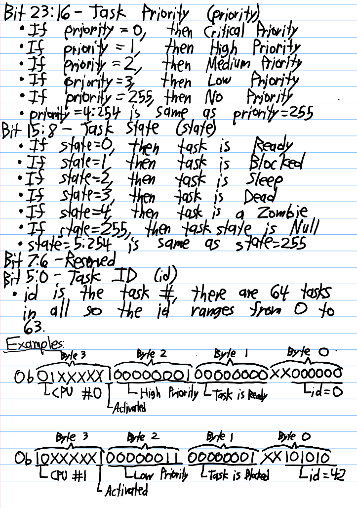
Task management is another major component covered by the Operating System, this includes the ability to manage every task. As mentioned, the OS has it's own memory to access that contains information about each task (the TCB Array). The TCB itself contains two 32-bit variables, the second one is the stack pointer for each task (a fixed value that get's designed upon initialization) and the first variable is the information about the task. Information includes CPU Core Allocation (CCA), activation state (does the task exist or not), task priority, task state, and the task id.
CPU Core Allocation:
- 00 - No Cores are Used
- 01 - Core 0
- 10 - Core 1
- 11 - Unused/Error
Task Priority* (priority):
- 0 - Critical Priority
- 1 - High Priority
- 2 - Medium Priority
- 3 - Low Priority
- 4:255 - No Priority
Task State (state):
- 0 - Ready
- 1 - Blocked
- 2 - Sleep
- 3 - Dead
- 4 - Zombie
- 5:255 - Null
Task ID (id):
- 0 - Task 0
- 1 - Task 1
- 2 - Task 2
- 62 - Task 62
- 63 - Task 63
...
* NOTE: The proposal for the priority variable will be changed depending on how the CPU scheduler will be implemented. Initially the CPU will be running with First Come First Served so priority isn't a factor anyhow, at least not yet.
3.3) CPU Setup
Wtih Memory Management and Task Management are two of the four important components for the Operating System, the next one is CPU Setup/Management. Of course the CPU also oversees the OS as well since the OS is running on the CPU (or one of the two CPU cores contained in the RP2040). At the beginning of the program, the Tasks and it's information as well as GPIO and the SysTick timer must all be initialized. The SysTick timer on each CPU core should be the last thing initialized since once the OS is done initializing, the OS will stay idle (will continuously run the NOP instruction on both CPUs until a SysTick later). Once the SysTick interrupt occurs the CPU will switch from the OS to the interrupt and start it's scheduling operations. There are multiple different scheduling options to pick from:
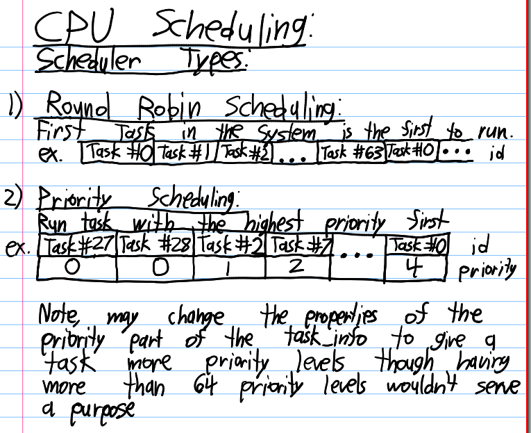
- First Come First Serve (FCFS): Scheduling system that takes the first task and runs it first (Task 0 in this case), then takes the second task (Task 1), until it reaches Task 63 and then resets to Task 0. One thing that makes this scheduling algorithm impossible is that there is a time limit on how long a task is allowed to run (0.5 ms, or ~66500 CPU cycles) so if a Task takes too long, it would have to move on to another task.
- Round Robin Scheduling: This scheduling system is similar to FCFS, except that this algorithm imposes a time limit known as the time quantum. The SysTick timer is the time quantum in this case so it falls into place. If a task takes too long to complete, the task is moved back into the queue to be used for later. This is the schedule I intend to target initially.
- Shortest Job First (SJF): This scheduling algorithm runs the quickest job first and then picks the next quickest. It's possible to implement this scheduling system if we can calculate how many CPU cycles each task ends up, but this won't be a part of this OS and wouldn't be compatible with FCFS nor Round Robin Scheduling anyhow, not to mention the next schedule.
- Priority Scheduling: Although similar to SJF, this one is distinct in that each job is assigned a priority value to each task. The higher priority tasks are the first ones to run whereas lower priority tasks are in queue to run later. This can be used in conjunction with the Round Robin scheduling for tasks that have equal priority. This method has a problem known as starvation where a task of low priority runs indefniitely, solution to this would be raising the priority after each SysTick until the OS decides it has to run.
So overall, the scheduling algorithm will be a mixture of Round Robin and Priority Scheduling with the Priority Scheduling taking precent (being the first) and the secondary algorithm with be Round Robin within the Priority Scheduler for tasks of equal priority. And if a task takes longer than a SysTick to run, the task has to pause (via SysTick) and the priority is set to 0 so the task can finish, though this maybe another later feature to implement.
3.4) GPIO Management
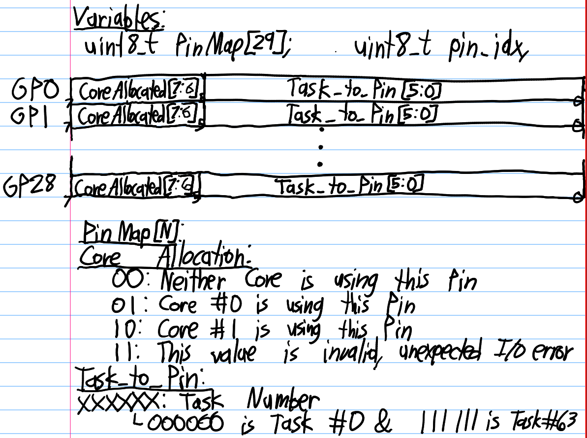
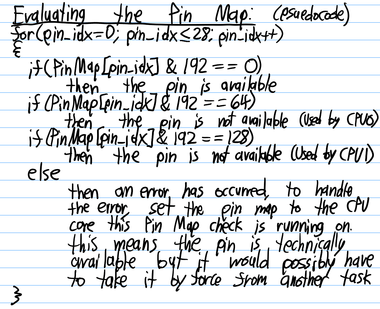
The first step for I/O management is to create the Pin Map, for each pin, an 8-bit integer will be assigned to it indicating two things. The first is which task is using the pin and second is which CPU core is using this pin. The first part of the variable is the most important one, the second one is probably not necessary if the TCB is already going to have information on which CPU core a task is going to run on. This information is still relevant since if a CPU core is already using the pin, it be best to not take it away from the task that needs it, though if an unexpected error occurs (PinMap[N]'s value is 0b11XXXXXX), then the OS is allowed to treat it as is the pin is not being used. Of course this kind of error shouldn't occur but it is a precaution for if it does. The last 6 digits indicate which task is using the pins (Task 0-63), which is straightforward. Should also note that both CPUs are also not allowed to access the same pin within a SysTick. This is due to both CPU cores likely going to run different tasks at a time and pins cannot output two things at once (like a light switch can't both be on and off).
With all of this we have all the basic components needed to build an operating system for the Raspberry Pi Pico/RP2040.
4) Programming the RPi Pico
4.1) Programming Tools
The Raspberry Pi Pico promotes using Python or MicroPython (written in C) for programming but for microprocessors, I intend to write the OS in the C programming language. It helps that was the language used when writing the OS for the ATmega328PB. Among the high level programming languages, C is the most effective for performing low-level operations. First step to setting up the Software Development Kit (SDK) for the Raspberry Pi Pico is to download the C SDK for it though here: https://github.com/raspberrypi/pico-sdk.git. Installation guide for installing the C SDK can be followed here: https://www.electronicshub.org/program-raspberry-pi-pico-using-c/. For debugging, the arm-none-eabi-gdb package will be essential in addition to the arm-none-eabi-gcc and arm-none-eabi-newlib packages, which is critcal for a project such as this one.
To make programming and debugging more elegent, an IDE is recommended, but actually setting it up is cumbersome and it's easier to just program using a text editor and the command line (text editors such as nano or Kate) and manually configure the system. I should note that this is not a comprehensive guide on how to create a software development setup for the Raspberry Pi Pico so I am omitting details on how I got things running on the software side of things. But a setup is definitely something to work on for Design Implementation.
4.2) Design Implementation
With the system set up it's finally time to implement the design that I created throughout this entire process. Of course to code everything on here at once would be foolish so rather I will be taking this step-by-step and do it by following procedures:
- A basic test application with two LEDs to see if the hardware and basic software
- Creating tasks and implementing the SysTick and TCB array.
- Implement Saving/Recovering Data to/from the Stack Memory.
- Implement Round Robin Scheduling and execute tasks on both CPU cores (but separate I/O for each one).
- Implement GPIO Permission system and Pin Map (two CPU cores and two tasks cannot share pins), then each task can have the two same pins and switch back and forth which task gets to use those pins.
- Change the CPU Scheduler to a Priority Scheduler with Round Robin as a secondary scheduler for tasks of equal priority.
- Design and then implement a Memory Sharing System.
There may be more ideas for the OS along the way but these will be things to work on for the time being.
4.3) Test Application
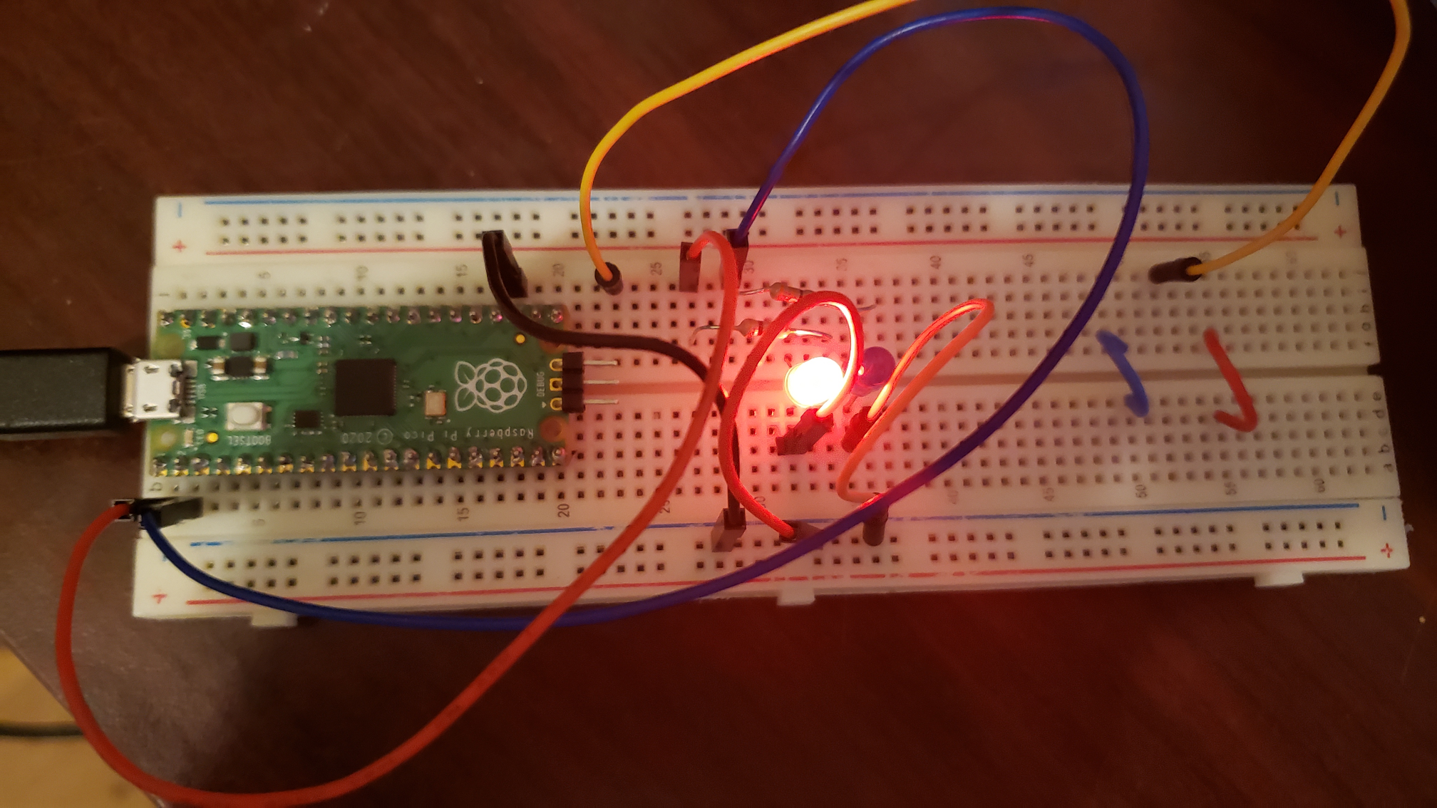
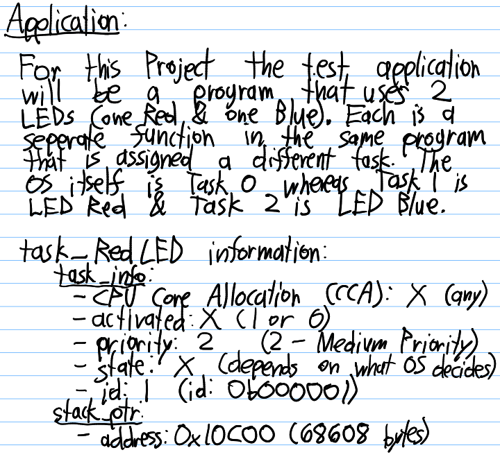
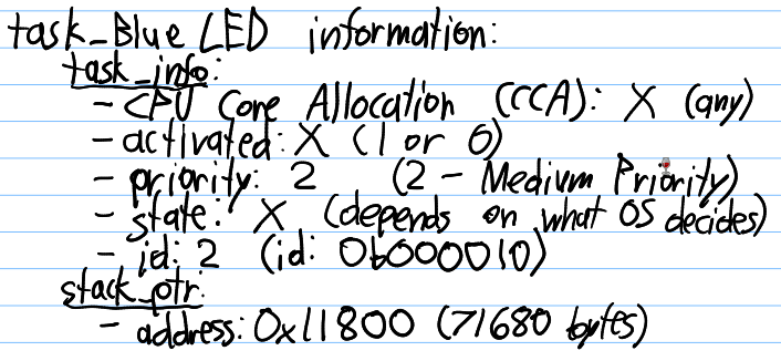
My test program here is a basic two LED setup. Both pins will be used for one task at a time since only one task is allowed to use the same pin/s at a time, but each task will output to the LEDs differently. The task_RedLED will have the red LED on and blue off and the task_BlueLED will have the blue LED on and red off. If this works then the result should be both LEDs acting accordingly and switching between red and blue. Once this test program works more complex setups can be designed in place since the same principles of OS design and GPIO sharing apply.
5) Conclusion
Although it took me a considerable amount of time to design the OS here, it took less time due to prior experience with designing an OS for an ATmega328PB which has far less RAM resources (2 kB vs the RP2040's 264 kB) and a single core CPU running at 20 MHz rather than a dual core 133 MHz processor. Once I come up with the initial code base it's gonna take time for me to decide on whether or not I want to upload this project on GitHub or attempt to create my own GitLab instance on the webserver and then upload it from there. I am hoping to go with the latter though it's less trivial to set up and my previous attempt to set it up failed. Once this is decided this project will receive an update.
6) References
ATmega328PB Datasheet: http://ww1.microchip.com/downloads/en/DeviceDoc/40001906A.pdf
RP2040 Datasheet: https://datasheets.raspberrypi.org/rp2040/rp2040-datasheet.pdf
ARM Cortex M0+ Devices Generic User Guide: https://www.keil.com/dd/docs/datashts/arm/cortex_m0p/r0p0/dui0662a_cortex_m0p_r0p0_dgug.pdf
Raspberry Pi Pico Datasheet: https://datasheets.raspberrypi.org/pico/pico-datasheet.pdf
Raspberry Pi Pico C SDK Installation Guide: https://www.electronicshub.org/program-raspberry-pi-pico-using-c/
Sections


Recent Posts
March 8, 2024: At last, the website has returned!
March 12, 2022: Note Binder - Note Organization Application: https://drewtechs.net/projects/note-binder
January 30, 2022: Updated Website with a new Web Server Setup.
October 15, 2021: Added Gitea to the Website to self-host source code: gitea.drewtechs.site
July 31, 2021: Project: Raspberry Pi Pico RTOS (DRPiTOS) Initial Design
June 1, 2021: Mini-Project: Portable Bluray Player
March 31, 2021: Added a Product Review for the Dell XPS 15 9575 w/Vega M
